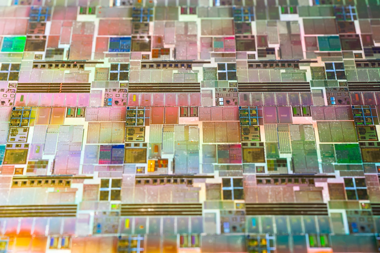
The silicon wafer method refers to the process of using silicon wafers as the fundamental substrate for fabricating semiconductors and integrated circuits (ICs). This method has been the backbone of the semiconductor industry for decades, powering the production of microchips used in everything from smartphones to computers, cars, and renewable energy technologies. The term encompasses multiple intricate processes, from crystal growth and wafer slicing to photolithography, etching, and doping, which ultimately produce the tiny transistors that make up modern electronic devices.
Overview of the Silicon Wafer Method
The silicon wafer method begins with raw silicon material and ends with the creation of complex semiconductor devices. It is a multi-step process that involves:
- Preparation of silicon wafers, which serve as the substrate for semiconductor manufacturing.
- Fabrication of microelectronics on the wafer surface through processes like photolithography, etching, doping, and deposition.
- Packaging and testing of the completed semiconductor devices.
This method has enabled the semiconductor industry to produce millions of transistors on a single chip, leading to exponential growth in computing power as described by Moore’s Law—the observation that the number of transistors on a chip doubles approximately every two years.
Key Steps in the Silicon Wafer Method
1. Silicon Purification and Crystal Growth
The first step in the silicon wafer method involves converting raw silicon (which is derived from silica in sand or quartz) into high-purity, single-crystal silicon ingots. This is essential because semiconductor devices require a pure and uniform crystalline structure to function properly.
- Raw silicon extraction: Silicon is extracted from silica through a reduction process in a furnace. The result is metallurgical-grade silicon, which is only about 98% pure.
- Refinement: The silicon is further refined to electronic-grade silicon (EG-Si) with a purity of 99.9999% or higher, often using a chemical vapor deposition process that involves converting silicon into trichlorosilane (SiHCl₃) and then decomposing it into pure silicon.
Once the silicon is purified, the crystal growth process begins.
a. Czochralski (CZ) Process
The Czochralski process is the most commonly used method for growing single-crystal silicon ingots:
- High-purity silicon is melted in a quartz crucible.
- A seed crystal, carefully oriented to ensure the correct crystalline structure, is dipped into the molten silicon.
- The seed crystal is slowly rotated and pulled upward, allowing the silicon to solidify around it in a perfect single-crystal structure.
- The resulting silicon ingot can be up to 1-2 meters long and vary in diameter from 100 mm to 300 mm or more.
b. Float Zone (FZ) Process
In the Float Zone process, a polycrystalline silicon rod is melted using a localized heat source, and a single crystal is grown as the molten zone moves along the rod. This method produces higher-purity silicon than the CZ process and is used for specialized applications requiring minimal impurities.
2. Wafer Slicing and Surface Preparation
After growing the single-crystal silicon ingot, the next step is to slice it into thin, circular wafers. These wafers will serve as the substrate on which microchips are fabricated.
- Wafer slicing: The ingot is sliced into thin wafers using a diamond wire saw. The thickness of these wafers typically ranges from 100 to 200 microns (0.1 to 0.2 mm).
- Lapping and polishing: The sliced wafers undergo lapping and chemical-mechanical polishing (CMP) to ensure they are perfectly flat and smooth. Even the slightest surface irregularities can disrupt the microchip fabrication process.
- Wafer cleaning: Wafers are thoroughly cleaned to remove particles, dust, and residues that might interfere with the manufacturing process.
3. Photolithography: Patterning the Wafers
Once the wafers are prepared, they are ready for the next step: photolithography, a key process used to transfer intricate circuit patterns onto the surface of the silicon wafer. This is where the individual components of a microchip, such as transistors, are created.
Photolithography involves several sub-steps:
- Coating with photoresist: A thin layer of a light-sensitive material called photoresist is applied to the surface of the wafer.
- Exposure: A photomask, containing the circuit pattern, is placed over the wafer. The wafer is exposed to ultraviolet (UV) light, which causes the photoresist to harden in areas that are exposed to light.
- Development: After exposure, the wafer is treated with a chemical developer that removes the unexposed (soft) photoresist, leaving behind the desired pattern.
- Etching: The patterned wafer is subjected to an etching process that removes the exposed areas of silicon, creating the circuit features.
Photolithography is repeated many times, each layer building different elements of the integrated circuit (IC).
4. Etching and Deposition: Shaping the Circuit Elements
After photolithography, additional processes like etching and deposition are used to further shape and form the components on the silicon wafer.
- Etching: In dry etching, plasma or reactive gases are used to remove specific areas of the silicon wafer. This process creates channels, trenches, or patterns in the silicon. Wet etching involves using chemical solutions to dissolve away the unwanted material.
- Deposition: Thin films of materials such as silicon dioxide (SiO₂), metals, or polysilicon are deposited onto the wafer surface. These layers form insulation, wiring, or other elements needed for the functioning of the microchip. Techniques for deposition include chemical vapor deposition (CVD) and physical vapor deposition (PVD).
5. Doping: Modifying Electrical Properties
Doping is the process of introducing small amounts of impurities into the silicon wafer to change its electrical properties. This step is critical for creating the p-type and n-type regions needed for transistors and other components.
- Ion implantation: Charged particles (ions) of boron, phosphorus, or arsenic are bombarded onto the wafer surface at high speeds. These impurities are embedded into the silicon crystal lattice, creating regions with specific electrical properties.
- Annealing: After doping, the wafers are heated in a furnace, a process known as annealing, to repair the crystal structure and activate the dopants.
6. Metallization: Creating Electrical Connections
Once the semiconductor structures (e.g., transistors, capacitors) are formed, the next step is to establish electrical connections between them.
- Metal layers: Layers of conductive materials like aluminum, copper, or tungsten are deposited onto the wafer surface using sputtering or CVD.
- Patterning: Photolithography and etching are again used to create the intricate patterns of metal interconnections (or interconnects) that link the various components on the chip.
7. Wafer Testing and Dicing
Before the wafer is processed further, it undergoes wafer testing, where each individual die (the area on the wafer that will become a microchip) is tested for functionality using specialized probes.
- Dicing: After testing, the wafer is cut into individual dies using a diamond saw. Each die represents a single microchip.
- Packaging: The individual dies are then packaged, which involves placing them into protective enclosures that provide electrical connections to external circuits and protect the chip from physical damage.
8. Final Testing
Once packaged, the chips undergo final testing to ensure they meet performance and reliability standards. The chips are tested for electrical performance, speed, and power consumption. Only those that pass the stringent tests are sent for integration into electronic devices.
Applications of the Silicon Wafer Method
The silicon wafer method is used to manufacture a wide range of semiconductor devices, including:
- Integrated Circuits (ICs): The microchips found in computers, smartphones, and other electronic devices are fabricated using silicon wafers. These ICs contain millions (or even billions) of transistors.
- Photovoltaic Cells: Silicon wafers are also used in the production of solar cells, where they convert sunlight into electrical energy.
- MEMS Devices: Microelectromechanical systems (MEMS), such as sensors and accelerometers, are made using silicon wafers. These devices are found in automotive systems, smartphones, and medical equipment.
- LEDs and Photonics: Silicon wafers are used in light-emitting diodes (LEDs) and other photonic devices for communication, lighting, and displays.
The silicon wafer method is the cornerstone of semiconductor manufacturing, enabling the creation of integrated circuits and microchips that power modern technology. From smartphones and computers to medical devices and renewable energy systems, silicon wafers serve as the essential building blocks of the digital age.
The complexity of the silicon wafer method, with its precise processes like crystal growth, photolithography, doping, and etching, highlights the intricate engineering and scientific advancements required to produce today’s advanced electronic devices. As technology continues to evolve, the silicon wafer method will remain critical in pushing the boundaries of computing,


